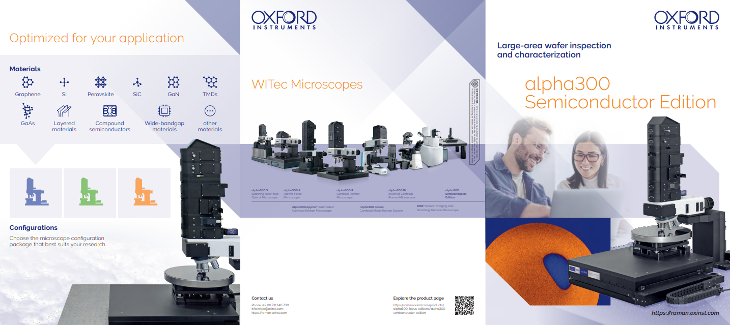
Large-area wafer inspection and characterization alpha300 Semiconductor Edition
Accelerate semiconductor analysis with industry-leading Raman and PL microscopy.
The alpha300 Semiconductor Edition is a precision-engineered confocal Raman and photoluminescence (PL) microscope, purpose-built for the detailed characterisation of semiconducting materials. Tailored for large-area wafer inspection, it delivers non-destructive imaging of crystallinity, defects, strain, and doping with scientific-grade accuracy.
Engineered with extensive automation, advanced vibration damping, and active focus stabilisation, this system ensures consistent, high-quality results even over full 300 mm wafers. TrueSurface technology maintains optimal focus during wide-area scans, enabling sharp, high-resolution imaging of surface and subsurface features.
By combining Raman and PL techniques, users can perform comprehensive 3D material analysis—ideal for research and quality control in both conventional and wide-bandgap semiconductors such as GaN, SiC, and perovskites.
Key Benefits:
- Large-area inspection up to 300 mm (12-inch) wafers
- Automated, high-throughput imaging workflows
- Surface, depth, and 3D imaging in one system
- Clear visualisation of strain, doping, and crystalline features
- Enhanced resolution with wavelength-optimised spectrometry
Explore how the alpha300 Semiconductor Edition transforms materials research and streamlines wafer characterisation—from the lab to the fab.
Please fill your information below to download the white paper.